Nanoimprint Lithography Facilitated Plasmonic-Photonic Coupling for Enhanced Photoconductivity and Photocatalysis (open access)
Vaibhav Gupta, Swagato Sarkar, Olha Aftenieva, Takuya Tsuda, Labeesh Kumar, Daniel Schletz, Johannes Schultz, Anton Kiriy, Andreas Fery, Nicolas Vogel, Tobias A. F. König*
Congratulations to Viabhav and Swagato (shared first authorship), as well as Olha and Daniel for their publication in Advanced Functional Materials. These PhD students were scientifically advised by Tobias König as first and second supervisor.
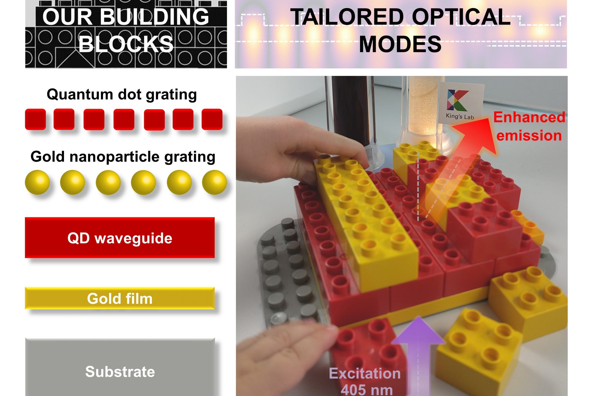
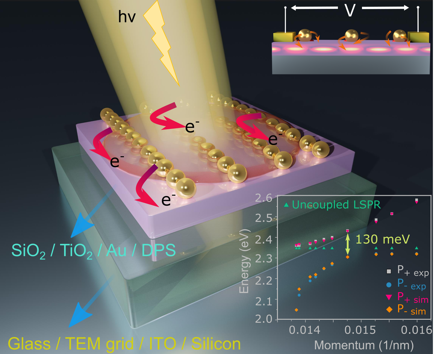
Imprint lithography has emerged as a reliable, reproducible, and rapid method for patterning colloidal nanostructures. As a promising alternative to top-down lithographic approaches, the fabrication of nanodevices has thus become effective and straightforward. In this study, a fusion of interference lithography (IL) and nanosphere imprint lithography on various target substrates ranging from carbon film on transmission electron microscope grid to inorganic and dopable polymer semiconductor is reported. 1D plasmonic photonic crystals are printed with 75% yield on the centimeter scale using colloidal ink and an IL-produced polydimethylsiloxane stamp. Atomically smooth facet, single-crystalline, and monodisperse colloidal building blocks of gold (Au) nanoparticles are used to print 1D plasmonic grating on top of a titanium dioxide (TiO2) slab waveguide, producing waveguide-plasmon polariton modes with superior 10 nm spectral line-width. Plasmon-induced hot electrons are confirmed via two-terminal current measurements with increased photoresponsivity under guiding conditions. The fabricated hybrid structure with Au/TiO2 heterojunction enhances photocatalytic processes like degradation of methyl orange (MO) dye molecules using the generated hot electrons. This simple colloidal printing technique demonstrated on silicon, glass, Au film, and naphthalenediimide polymer thus marks an important milestone for large-scale implementation in optoelectronic devices.